

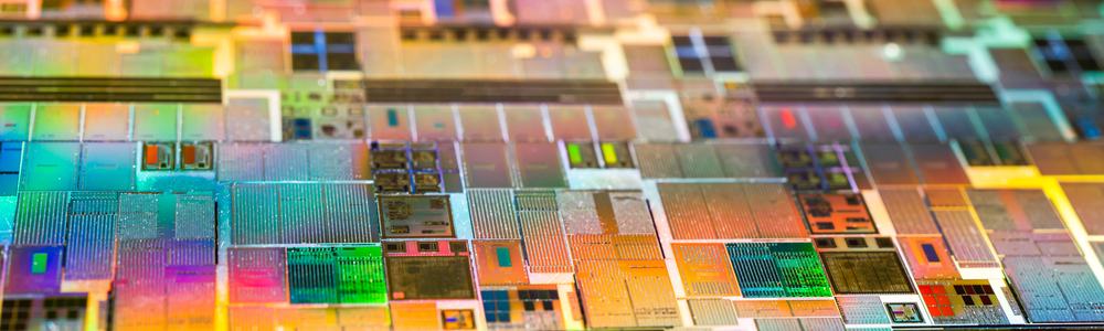
Researchers at the National Institute of Standards and Technology (NIST) achieved a breakthrough in the development of photonic chips, potentially cracking the means to make tiny photonic integrated circuits capable of operating in extreme environments.
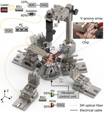
The development, detailed in a newly published paper in the Photonics Research journal, saw the researchers overcome the packaging challenge of reliably attaching an optical fiber to a photonic chip.
While traditionally used adhesives like organic polymer glues tend to crack or degrade when exposed to extreme cold, heat, or radiation, NIST scientists employed a sodium hydroxide solution to fuse surfaces at the molecular level.
Using a technique originally developed by NASA called hydroxide catalysis bonding (HCB), the researchers created a glasslike chemical bond between the optical fiber and the photonic chip that formed a more rigid, stable connection.
Despite bombarding HCB-packaged photonic chips with intense radiation, subjecting it to vacuums, and exposing them to intense temperatures, the hardware “remained intact.”
“Our study marks a major step toward bringing the speed and efficiency of photonics into environments where conventional semiconductor chips powered by electric current and photonics chips packaged using traditional methods have not been able to operate,” NIST physicist and project lead Nikolai Klimov noted in the paper.
Increasingly seen as the next frontier in semiconductors, photonics is a concept that sees chips convey information using light instead of electricity at far faster speeds while consuming considerably less power compared to conventional hardware.
It’s a technology that’s already a reality in the networking world, providing copper-alternative connections in switches like Nvidia’s upcoming co-packaged optics line or Celestial’s Photonic Fabric platform, a vendor that was recently acquired by Marvell Technology.
The idea of light-based connectivity is also seen as a potential boon for use in space-based deployments, providing interconnectivity between satellites in orbit, among other potential applications. But to bring the idea of space-faring photonics to life, the hardware needs to be able to work in a vacuum and handle the intense radiation from cosmic rays and solar flares.
Where traditional packaging processes would fail to make reliable connections in such an environment, the NIST team’s use of HCB resulted in a packaging method that provided “exceptional resilience across a remarkably wide environmental range.”
High-temperature testing was not performed directly on the packaged photonic chip due to limitations of the commercial optical fibers available. However, the researchers performed additional studies on their HCB-based photonic packaging and determined that it remains mechanically stable at temperatures far higher than what conventional adhesives can withstand.
“This approach creates a bond that is as resilient as the optical fiber itself,” Klimov wrote. “It allows photonic integrated circuits to go places they simply couldn’t go before.”
The process wasn’t without its flaws, chiefly that the bonding process requires “several days to complete.”
But the research team viewed the production timeline as “an engineering issue rather than a fundamental barrier,” contending that with more focused development, engineers could dramatically shorten the packaging time to make the HCB technique suitable for large-scale manufacturing.
The NIST efforts are the latest in a growing number of photonic breakthroughs as the technology’s potential inches ever closer.
In November last year, New York University scientists uncovered a material called "gyromorphs" that is better than any other known structure at blocking light from incoming angles – meaning it could potentially control optical properties.
Just a month earlier, researchers at Japanese giant NTT created what they claim is the world’s first chip that rewrites itself using light patterns – delivering a huge blow to the traditional “one device, one function” paradigm.





Comments