


Huawei’s Connect event last week saw the vendor double down on AI hardware offerings, along with plans for clusters comprised of thousands of its own chips. Central to powering these “supernodes”, however, is a scale-first strategy where the vendor focuses initially on connecting hardware together before boosting the power and precision of its hardware.
At its event in Shanghai, the Chinese giant unveiled UnifiedBus 2.0, a new interconnect protocol set to act as the backbone of its next-gen cluster.
According to Huawei Rotating Chairman Eric Xu, the firm has been working on the protocol since 2019 because it didn’t have access to advanced process nodes following U.S. sanctions on AI chip exports to China. Against a backdrop of trade restrictions, Huawei opted to focus on innovations in connecting chips rather than building faster individual processors.
“With UnifiedBus, we're able to interconnect computing resources on a massive scale,” Xu said during his keynote, with Huawei planning to open source version 2.0 of the interconnect protocol and build an ecosystem around it.
UnifiedBus 2.0 delivers TB/s-level bandwidth and 2.1-microsecond latency across interconnected chips, enabling what Huawei called “bus-grade interconnect.”
In terms of protocol details, Xu outlined during his keynote that reliability was built into “every layer” of UnifiedBus 2.0. He suggested there is 100-ns-level fault detection and protection switching on optical paths to ensure applications continue to run normally even if faults occur.
Beyond protocol developments, Huawei has overhauled its optical components, modules, and interconnect chips. Although design specifics weren’t disclosed, the Huawei chairman said the enhancements have led to a hundredfold increase in the reliability of its optical interconnects and extended device range to more than 200 meters.
‘A new paradigm for large-scale compute’
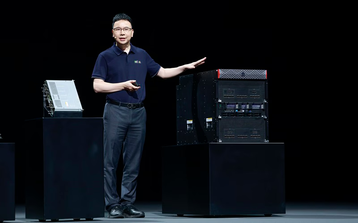
Huawei wants its interconnect protocol to help turn thousands of distributed processors into a single logical machine. It’s set to support Huawei’s next generation of supernode offerings, such as the Atlas 950 SuperPoD, which is scheduled for fourth-quarter 2026.
Capable of scaling up to 8,192 Ascend 950DT chips, Huawei claims the Atlas 950 packs 6.7 times more compute power than Nvidia's forthcoming Vera Rubin NVL144 platform. Using Huawei’s UB-based network architecture, it supports intra-board, cross-board, and inter-rack full-mesh NPU interconnections, reportedly offering 1.7 petabytes per second (PB/s) of memory bandwidth in a single rack.
We’ve already seen a glimpse of an earlier iteration of the protocol, with UB1.0 supporting Huawei’s answer to Nvidia’s GB200 NVL72, the CloudMatrix 384.
That system packs five times more chips than Nvidia's rack-scale rival, while, in turn, consuming roughly four times the power.
While power consumption challenges might have put off potential users in the past, Xu argues that its interconnect innovations could prove valuable even for systems using more advanced chips.
The company's roadmap revealed at Huawei Connect showed annual chip releases through to 2028, with doubled performance each generation – suggesting confidence that the vendor’s scale-plus-connectivity approach will remain viable as its individual chip capabilities improve.
“[UnifiedBus] deeply interconnects physical servers so that they can learn, think, and reason like a single logical server,” said Yang Chaobin, Huawei's Board director and CEO of its ICT business group. “This has created a new paradigm for large-scale compute that is more efficient, reliable, and scalable.”






Comments