

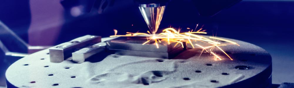
Researchers from the National Institute of Standards and Technology (NIST) developed a new 3D printing approach for metal alloys, providing a glimpse into the potential future of hardware production.
NIST engineers were looking into ways to improve metal 3D printing. Conventional approaches build parts layer by layer via laser tracing straight lines from digital models.
Outlined in the Additive Manufacturing journal, the researchers instead sought to employ a laser that draws loop-the-loops, physically stirring molten metal puddles that were “smaller than a ladybug’s eye.” Due to a lack of heat in that puddle, the alloys were essentially tricked into mixing, allowing the NIST team to combine metals and thereby creating 3D structures far more easily.
“Commercial 3D printer software can’t make these patterns,” NIST researcher Ho Yeung explained. “They are very limited in how the laser’s path can be adjusted, so we had to write the software from scratch.”
This concept doesn’t require any new major parts, allowing existing metal 3D printers to be programmed to use this technique. To verify their success, the research team also developed a way to watch changes in the metal using X-rays as they melted, ensuring solidification occurred in a fraction of a second.
The simple concept comes at a time of great supply chain consternation, with hardware manufacturing a painstaking process that requires vast amounts of metals, among other components. For example, copper demand is expected to surge by 50% while supply faces a projected supply deficit of 10 million metric tons by 2040.
NIST’s concepts could dramatically reduce cost and inventory complexity for manufacturers, with suppliers able to mix alloys on the fly while meeting intense material demands.
While such an idea wouldn’t work for producing silicon dies – as they require intense precision using photolithography and etching, among other intricate processes – the surrounding ecosystem could be in line to benefit. For instance, thermal management components made from high-entropy alloys (HEAs) that are used in chip packaging and heat spreaders could be more easily created. Or fab equipment parts that must withstand corrosive environments and extreme temperatures; superior alloys would minimize the operational downtime currently experienced by semiconductor manufacturers.
The technique is, of course, still early stage, but the team at NIST believes it has the potential to reduce material costs, going as far as to suggest future applications could see the blade of a jet turbine “3D-printed out of several different metals without the need for welding, which might create weak spots.”
“We want to accelerate alloy making,” Yeung added. “Metal 3D printing has the potential to make parts that used to be impossible.”
NIST’s efforts around 3D printing, otherwise known as additive manufacturing (AM), are already finding real-world applications at the heart of chip production.
Dutch company ASML, which uses lithography machines to manufacture advanced semiconductors, has quietly been integrating AM throughout its systems, with more than 200 printed parts now in production.
A 2023 paper revealed the company has used the technology to redesign cooling channels that improved thermal performance sixfold, and to cut the production time of a critical titanium wafer stage carrier by a factor of three, while reducing associated CO2 emissions by 60%.






Comments