


Scientists at MIT developed the means to produce flexible and transparent chips to bring silicon photonics to wafer-scale.
Conventional silicon photonic development has been limited to fabrication processes on the individual device or at chip-scale, thereby limiting potential scalability. Detailed in the journal Optica, the research team sought to overcome this through optically transparent and mechanically flexible silicon photonics wafers.
The scientists managed to develop a 300-millimeter silicon-photonic platform both entirely transparent and capable of withstanding “thousands of bends” without optical performance degradation.
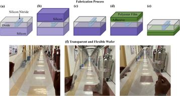
A single chip was bent a total of 3,000 times, with around 500 bends performed at each bend diameter, without any noticeable performance impact on the device. The researchers observed that unlike severe fractures that occur if a typical rigid silicon photonics chip is bent, cracks in their flexi-wafer concept “initially do not lead to major waveguide misalignment or scattering.” Failure only really occurred when the hardware was subject to “an aggressive bend diameter” of 0.08 inches, or about that of a toothpick.
The fabrication process was developed in collaboration with non-profit semiconductor research firm NY Creates. It sees waveguides that guide light similarly to how copper wires guide electricity in conventional hardware placed on a silicon substrate. A temporary silicon wafer is then bonded for structural stability and flipped, with the original piece removed. Engineers then bond a transparent and flexible substrate onto the exposed oxide surface before removing the temporary silicon handle wafer, which results in the transparent wafer with fabricated silicon photonics.
Essentially, their foundry process works like applying a double-sided decal: building intricate layers on a rigid backing, temporarily tape the top for stability while you peel off the original base, before sticking the exposed layers onto a flexible film and then removing them.
A total of six 300-millimeter wafers were made using the method, with the researchers touting it as a means to scale silicon photonic hardware. Their paper suggests the concept could be applied to tech like wearables, including health care monitors or curved augmented reality for eyeglasses or a pilot’s helmet.
While the research paper focused more on applying the technology to wearables, flexible, micro-thin silicon photonic wafers could break standard data center rack designs. Imagine wafer designs that could theoretically be rolled into a cylinder or contoured around a specialized 3D liquid-cooling core.
“Because we are using stable 300-millimeter foundry fabrication tools, we can design systems with a very large number of devices and feel confident that they are going to perform up to specifications, which is extremely important,” lead author Tal Sneh told MIT News.
The idea is still being fleshed out, so don’t expect any flexible wafer-scale chips from Cerebras any time soon.
The researchers want to improve the platform, with plans to add active modulation and metallization in the hopes of enabling higher-temperature processing steps to reduce waveguide propagation loss and further boost performance.






Comments