


Broadcom commenced shipments of an apparent industry first in the form of two-nanometer (nm) custom compute system on chip (SoC).
Built on the chip giant’s 3.5D eXtreme Dimension System in Package (XDSiP) platform, the offering marks Broadcom's opening of the door to its custom chip clients ready to produce iterations of their 2nm designs, with transistor placement getting ever-denser to pack the most out of hardware.
Debuted back in 2024, Broadcom’s 3.5D XDSiP packaging approach sees it stacking multiple dies together in a single package rather than relying on one monolithic chip.
Where the previous industry standard of 2.5D integration relied on multiple chiplets sitting side-by-side on an interposer substrate, that approach could only really integrate up to 2,500-square-millimeters (mm2)of silicon and around eight high bandwidth memory (HBM) stacks in one package.
But with the sheer computing power required to handle AI training and ever-growing inference workloads, Broadcom’s 3.5D instead places dies directly on top of another, allowing chips to feature more than 6000mm2 of silicon and up to 12 HBM stacks.
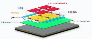
Broadcom positions its packaging tech to custom chip customers as a means to boost compute, memory, and networking components, with signals traveling far shorter distances and thereby reducing both latency and power consumption.
Die stacking, though, is not a new production approach to boost transistor density – Intel and Taiwan Semiconductor Manufacturing Co. (TSMC) are believed to be working on their own iterations of 3D stacking architectures.
Broadcom’s Face-to-Face bonding concept, meanwhile, takes the idea of 3D stacking and combines it with 2.5D packaging, orienting both dies so their active circuitry faces inward toward each other rather than one facing the back of the other like the older Face-to-Back (F2B) approach. This new approach is said to enable far denser connections with lower electrical interference and greater mechanical strength.
“Since introducing our 3.5D XDSiP platform technology in 2024, Broadcom has expanded its 3.5D platform capabilities to support XPUs for our broader customer base that will ship from [the second half of 2026],” Frank Ostojic, SVP and GM of Broadcom’s application-specific integrated circuit (ASIC) products division, noted. “These developments underscore Broadcom’s unrivaled technology leadership in delivering high-complexity XPUs to enable transformative breakthroughs in AI.”
The recipient of its first 2nm custom hardware is Fujitsu as part of the Japanese giant’s Fujitsu-Monaka project. Set for release in 2027, Fujitsu’s next generation of custom high-performance computing (HPC) hardware comprises Arm-based designs and is set to power FugakuNEXT, the next-generation of its flagship supercomputer and formerly fastest system in the world.
“By combining 2nm process innovation with Face-to-Face 3D integration, it unlocks unprecedented compute density and energy efficiency essential for the next era of AI and HPC,” Naoki Shinjo, SVP and head of the advanced technology development unit at Fujitsu, explained. “This breakthrough is a key enabler for Fujitsu’s Fujitsu-Monaka initiative to deliver cutting-edge, high-performance, and low-power processors.”
In addition to Fujitsu, Broadcom counts a host of big names it already supplies custom silicon for, including OpenAI, Anthropic, and TikTok parent ByteDance. It’s also helped develop each of Google’s seven generations of Tensor Processing Units (TPUs), including its latestIronwood generation.
Getting smaller, getting faster
The exponential shrinking of hardware – chip miniaturization – is, of course, nothing new, with overarching principles like that of Moore's Law, named after the late Intel co-founder Gordon Moore. That law posits that the density of transistors on a chip doubles roughly every two years, and by virtue, increases performance.
Where chip manufacturers like Broadcom were producing XPUs at the 7nm back in 2018, that shrunk down to 3 nm by 2022. And producers are gearing up to take density to the next level.
Marvell Technology was also an early player in the market, having debuted a custom static random-access memory (SRAM) solution on the 2nm process.
Intel has begun working on 2nm equivalent – 18 angstrom (A) – which is believed to be in risk production. TSMC has also made steps toward production, despite its customers' penchant for 3nm.






Comments