

AI infrastructure is hitting a power wall, and Microsoft believes the solution lies in technology borrowed from smartwatch displays.
While power efficient, traditional copper links have a limited reach of around two meters, optical links such as fiber optics can reach longer distances, but at the expense of high power consumption and lower reliability.
Microsoft researchers sought to bridge the gap between the two with “Mosaic," a prototype interconnect system capable of maintaining high network speeds across longer distances, while using far less power.
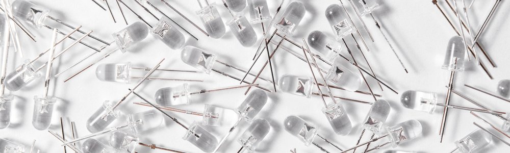
Detailed in a paper published at the recent ACM SIGCOMM event in Portugal, Mosaic makes use of directly modulated microLEDs – a technology originally developed for screen displays – instead of lasers.
Due to their small size, microLEDs can be modulated at several gigabits-per-second and are placed in large groups, or arrays. A typical smartwatch, for example, would feature more than half a million microLEDs, and their simple structure and temperature insensitivity make them more reliable than lasers.
Microsoft engineers sought to leverage the technology in an “optical wide-and-slow architecture” – switching from a small number of high-speed serial channels towards hundreds of parallel low-speed channels.

For copper or traditional optical technologies, a wide-and-slow approach would be highly impractical due to electromagnetic interference in the former, and the sheer cost and power consumption brought on by the latter tech.
Microsoft's Mosaic approach, however, employs microLEDs, which, while operating at lower speeds, massively improve power efficiency by eliminating the need for complex electronics and reducing optical power requirements. The concept also enables reach to be greatly extended, reaching distances of up to 50 meters, compared to just two meters.
“Mosaic achieves 10× the reach of copper, reduces power consumption by up to 68%, and offers 100× higher reliability than today’s optical links,” the researchers wrote. “By overcoming the reach, power and/or reliability limitations of existing link technologies, we hope that Mosaic will also act as an enabler for many recently proposed (and hopefully new) topologies and architectures for next generation of data center and AI clusters.”
In addition, microLEDs wouldn’t take up much space, with a potential 800 Gb/s Mosaic link capable of being developed using a 20 millimeters by 20 millimeters (20x20) microLED array – meaning it would fit on a die less than one millimeter by one millimeter.
Microsoft’s Mosaic concept wouldn’t require cluster operators to rework their stack, with the tech being fully compatible with today’s pluggable transceivers’ form factors. It’s also protocol-agnostic, as it simply relays bits from one endpoint to another, meaning it’s compatible with everything from Ethernet to PCIe, as well as proprietary systems like Nvidia’s NVLink.
In a blog post outlining the technology, Paolo Costa, a Microsoft partner research manager, stated that the company was collaborating with its suppliers to “productize” Mosaic and scale it for mass production, though it’s far from becoming a reality in the short tun.
Overcoming the technical hurdles
While conceptually simple, getting a technology traditionally used to display images on consumer devices to transmit data posed several challenges for the researchers. Microsoft employed a multidisciplinary team spanning expertise across integrated photonics, lens design, optical transmission, and analog and digital design to bring Mosaic to life.
For example, the team employed imaging fibers, which can support thousands of cores in a single fiber, rather than using individual fibers per channel, which would have been exorbitantly expensive and complex.
Further compounding development was the fact that microLEDs are a less pure light source, with larger beam shapes and a broader spectrum. The Microsoft team overcame this by employing an optical lens design and “a power-efficient analog-only electronic backend, which does not require any expensive digital signal processing.”
Tests of a prototype Mosaic saw the concept transmitted across 100 channels – 25 channels simultaneously, with each channel transmitting at 2 Gb/s over 20 meters.
According to Costa, Mosaic can help save the equivalent power of more than 10-watts per cable while reducing failure rates by up to 100x.
“With global annual shipments of optical cables reaching into the tens of millions, this translates to over 100 [megawatts] of power savings per year, enough to power more than 300,000 homes,” Costa added. “While these immediate gains are already significant, the unique combination of low power consumption, reduced cost, high reliability, and long reach opens up exciting new opportunities to rethink AI infrastructure from network and cluster architectures to compute and memory designs.”




Comments