


The memory shortage, or to go by the more widely used nom de guerre of RAMageddon, has seen component prices skyrocket, lead times for hardware extend to the end of the decade, and cascaded into non-volatile (NAND) flash, solid state drive (SSD), and, more recently, motherboards.
Conceived around the same time Sandisk was nswer may have arisen, at least in the sense of breaking the fundamentals of memory we know today. Memory chip maker Sanddisk has been steadily developing what it thinks can break the stranglehold of high bandwidth memory (HBM), shifting from a compute-memory gap to a memory-centric architecture: high bandwidth flash, or HBF.
Conceived around the same time Sandisk was spun out of Western Digital, HBF essentially takes the best NAND flash – improved capacity – and combines it with the ultra-wide, stacked architecture of HBM. The result? Up to 16-times the capacity of HBM while delivering comparable bandwidth, all while maintaining a similar price point.
Such a concept could allow operators to attach terabytes of memory to graphic processing units (GPUs) thereby vastly reducing the physical footprint and power consumption of AI clusters. As a result, it caught the attention of Google researchers, who, in a paper published around the turn of the year, suggested HBF could deliver as much as 10-times the memory capacity per node.
Before you get too excited, it’s important to note that Sandisk doesn’t expect the first inference devices powered by HBF to sample until early 2027. But that hasn’t stopped the company from gearing up for its eventual arrival.
Earlier this year, Sandisk teamed with SK hynix to standardize HBF via the Open Compute Project (OCP) in an effort to make it easier to integrate and broadly adopt upon its eventual release.
Cynthia Hsu, senior director for design engineering at Sandisk, framed the joint effort as enabling ecosystem-wide, compatible, scalable adoption, not something done in a silo.
“The first generation can still be a 2.5D integration, so you can keep your same cooling [and] thermal methods. And NAND actually has the benefit that we can go to higher temperatures,” Hsu said.
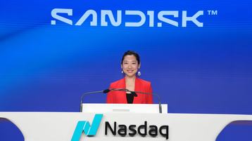
Speaking to SDxCentral, the Sandisk executive explained the choice to collaborate with OCP, stating, "We feel it will allow us to move a little bit faster."
“You don't want to do this in a silo. And we're moving quite fast under OCP," Hsu added. "Actually, you won't have to wait too long.”
How exactly can HBF smash the AI memory wall?
To understand why HBF matters, you need to understand what's actually constraining AI inference today.
Arguably, one of the main problems with AI is the sheer size of models. The "bigger is better" way of thinking has led to some mammoth frontier systems such as the 405 billion parameter Llama 3.1 from Meta or DeepSeek-V3.2, or even OpenAI models that can run parameters in the trillions. But in turn, this has led to massive demands on both bandwidth and capacity, ultimately forcing compute bills to routinely skyrocket – and yet the phenomenon of "tokenmaxxing" shows no signs of slowing.
Hsu and the team at Sandisk contend that traditional HBMs, which use dynamic random-access memory (DRAM) at their core, cannot scale physically or economically.
Where central processing units (CPUs) and GPUs have improved at roughly exponential rates, memory has taken a much slower route. If computing power outpaces data delivery, GPUs endlessly idle, which is incredibly expensive and inefficient.
The sheer memory requirements for some of the largest models make that wall even higher. Take Llama 3.1, which at 16-bit floating-point (FP16) you’d need around 810 gigabytes (GB), a figure that drops to 405 GB if running at FP8. No single GPU has that much HBM, so weights get sharded across many chips and the interconnects between them become the next bottleneck.
The argument for HBF is what if we traded some latency for a dramatic jump in capacity while keeping bandwidth competitive?
“For AI inference workloads, what you’re really doing is streaming the model weights to the accelerator," Hsu explained. "So it’s a very read‑intensive workload where you can often pipeline and sequence your reads. … What really matters is bandwidth more than latency."
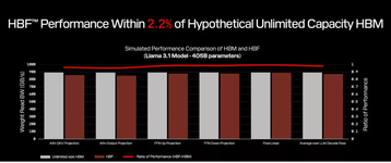
“We took NAND, redesigned it, and optimized it for high bandwidth through parallelism. And with NAND, we can deliver high capacity, Hsu added. "So with this, we uniquely combine very high bandwidth with massive capacity, and then we purpose-built this for AI inference workloads.”
Beyond slashing latency, Sandisk is positioning HBF as a means to reduce energy consumption for memory-intensive workloads. Hsu outlined that once DRAM starts to hit temperatures of around 80 degrees to 85 degrees Celsius (176°F to 185°F), it starts “bit flipping” – unintentionally causing the data stored in the memory cells to leak and change state.
“NAND is reliable; it can go to very high temperatures, much higher than DRAM,” Hsu added. “It's also non-volatile, so if you saved your trained model in HBF, you don't have to keep refreshing it and that saves you power as well.”
A distinct memory category for disaggregated inference
While HBF is some ways off from breaking down the memory wall, Sandisk got almost an early validation in their efforts from this year’s Nvidia GTC event when the flagship announcement was the Groq language processing unit (LPU), heralding the displacement of HBM in favor of static RAM (SRAM).
Add to that the meteoric rise of wafer-scale chip maker and SRAM proponent Cerebras, which has since secured deals with Amazon Web Services (AWS) and OpenAI.
For Hsu, the shift validated something Sandisk had already been thinking through: Modern AI inference isn't a monolithic workload, instead splitting into a compute-heavy prefill phase and a memory-bound decode phase. Hsu argues that disaggregated architectures, where different memory types handle different stages, are the logical response.
“You could use HBM for the more compute-heavy side and build a separate system that is more memory-bound, then you use HBF for that,” Hsu said. “This is aligned to where people are already looking at disaggregated inference.”
The broader significance, Hsu contends, is that HBF isn't simply a better version of existing memory, but a distinct memory category. Previously, architects had to pick from what was available and design their software around those constraints. HBF changes that calculus entirely.
“[HBF] uniquely combines high bandwidth with high capacity. So now you have another option that you can actually optimize for,” Hsu added.
From hyperscalers to startups: HBF's road ahead
While both HBF and its related standard are some way off, the team developing it has already got one eye on the road ahead. For Hsu, that confidence stems from something more fundamental than a simple product roadmap. As HBF is built on NAND, which is viewed at the most scalable semiconductor technology in existence (to date), it means capacity gains don’t and won’t stop at the first generation.
“It's not a 10-year-out project. It's not like we're researching new materials. NAND has a roadmap to keep scaling, and with HBF being a NAND-based technology, you're reaping the benefits of those gains,” Hsu said.
Sandisk’s HBF concept is built on the company’s own complementary metal-oxide-semiconductor (CMOS) directly bonded to array (CBA) wafer bonding technology. Here, CMOS control circuits, which perform logic functions, and cell array wafers are fabricated independently, only to then be bonded together – a 3D flash memory process that results in faster operation speeds and lower power consumption.
Already used in the company’s BiCS NAND product, which it co-developed with Kioxia, engineers are taking this same process to HBF to squeeze more out of the underlying flash. As Hsu explained, fabricating the CMOS and array wafers separately and bonding them later “brings you the best cell performance and the best CMOS I/O performance as well,” exactly what you want for a low‑latency, high‑bandwidth memory device that still rides the existing NAND scaling roadmap.
The upshot, Hsu argues, is that HBF isn't just a solution for the hyperscalers and cloud giants currently buckling under the weight of their own AI ambitions. Smaller neoclouds and startups priced out of massive HBM clusters stand to benefit just as much, perhaps more so.
“It will enable big and small, everyone," Hsu said. “Less capital, less power.”
For an industry that has spent the past few years treating memory as an afterthought and instead fawning over shiny GPUs, Hsu and the team at Sandisk make quite a radical proposition. Only time will tell if the memory wall may finally have met its match.




Comments