


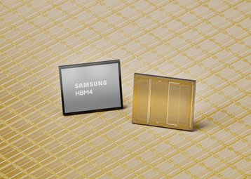
Samsung has commenced mass production on its next-generation high bandwidth memory (HBM) product, HBM4.
According to Samsung, the firm leveraged its 6th-generation 10 nanometer (nm)-class dynamic random access memory (DRAM) process (1c) for the chip, in contrast to its rivals, who instead stack DRAM dies on a passive interposer, a thin silicon layer that routes signals between the memory and GPU. In place of the logic die of the sort used by Samsung, the GPU or accelerator handles the logic within its rivals’ manufacturing setup.
Samsung claims its HBM4 delivers a sustained processing speed of 11.7 GB/s, about 46% higher than the current 8 Gb/s standard. This corresponds to a 1.22-times improvement over the previous generation HBM3E, which topped out at a 9.6 Gb/s pin speed. The HBM4’s throughput can also be scaled up to 13 Gb/s, which Samsung said would alleviate the current data bottlenecks hitting AI model development.
Per-stack total memory bandwidth has increased by 2.7-times versus HBM3E, reaching up to 3.3 Tb/s. With 12-layer stacking, Samsung is offering HBM4 in capacities from 24 gigabytes (GB) to 36 GB, and plans to support future customer schedules with 16-layer stacks, extending capacities up to 48 GB.
To cope with the power and thermal impacts of doubling data input/output (I/O) pins from 1,024 to 2,048 pins, the South Korean giant embedded low-power design techniques into the core die. By using low-voltage through-silicon via (TSV) technology and optimizing the power distribution network, its HBM4 reportedly delivers a 40% gain in power efficiency, while also improving thermal resistance by 10% and heat dissipation by 30% compared with HBM3E.
“Instead of taking the conventional path of utilizing existing proven designs, Samsung took the leap and adopted the most advanced nodes like the 1c DRAM and 4nm logic process for HBM4,” Sang Joon Hwang, EVP and head of memory development at Samsung Electronics, explained. “By leveraging our process competitiveness and design optimization, we are able to secure substantial performance headroom, enabling us to satisfy our customers’ escalating demands for higher performance, when they need them.”
2026 going into 2027 – and beyond
Anticipating that its HBM sales will more than triple in 2026 compared to last year, Samsung expects sampling for HBM4E to begin in the second half of 2026, with custom HBM samples reaching customers in 2027, aligned to their individual specifications.
Nvidia is likely to be in this tranche, reportedly being close last month to giving Samsung approval for part of its HBM4 needs in service of Nvidia’s next-gen Rubin GPUs. Samsung will reportedly supply half of the small outline compression attached memory module 2 (SOCAMM2) that Nvidia requires for Rubin mass production.
According to a Digitime report from November, Samsung expected to allocate up to 150,000 wafers per month of 1c DRAM capacity to HBM4 by the end of 2026, including 80,000 wafers of new 1c capacity and converted portions of older DRAM lines.
In remarks reported by Reuters, Jai-hyuk Song, CTO of Samsung’s Device Solutions, claimed that corporate customers who’d already got their hands on some HBM4 shipments have hailed the chip’s performance as “very satisfactory.”
The firm also attributed its HBM4 success to tight integration between its foundry and memory businesses, while planning to broaden its partnerships with global GPU manufacturers and hyperscalers for next-generation application-specific integrated circuit (ASIC) development.
According to reports, Samsung is already onto its next play, developing a version of HBM that integrates a computing core, effectively HBM with processing-in-memory (PIM) or compute-enabled memory. According to Song, the new HBM design can deliver up to a 2.8-times performance boost while maintaining the same level of power efficiency.
The firm is also working on custom HBM (cHBM), an ASIC that maximizes performance through customization for AI semiconductor customers, plus zHBM, which sees DRAM dies layered vertically along the z-axis to achieve massive capacity and speed in a compact footprint.
Song claimed PIM is being applied to its low-power double data rate 5X (LPDDR5X) output, a low-power DRAM primarily designed for mobile and edge devices, with the firm also developing a standard for LPDDR6.


Comments