

Nvidia unveiled a custom die base aimed at accelerating memory bandwidth for custom silicon linked with its hardware.
Dubbed NVHBM, the base-die innovation ties in with NVLink Fusion and extends its high-speed NVLink backplane technology to partner specialized custom processing units (XPUs). It allows for increased memory bandwidth with high-bandwidth memory (HBM) when linking non-Nvidia accelerators with Nvidia hardware in rack-scale solutions.
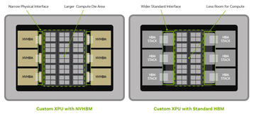
NVHBM sees memory controllers integrated directly into the 3D HBM stack instead of directly on the XPU board, a decision Nvidia contends brings up to 30% more memory bandwidth compared with standard high-bandwidth memory generation 4 (HBM4e) and as much as 15% lower power consumption.
By removing HBM from the physical layer of the XPU it also widens the compute area, allowing for partner silicon designers to pack more power onto their devices.
“Shrinking the memory interface connections enables the central AI compute die to expand into the newly freed space,” an Nvidia technical blog reads. “This reclamation provides up to a 30% increase in available main-die silicon for compute or other features. The additional silicon area enables XPU designers to add more capabilities within a fixed package footprint. These improvements can help custom XPUs support larger models, read KV cache data faster, and improve training and large-scale inference.”
Amazon’s custom silicon arm, Annapurna Labs is among the first partners to sign up for NVHBM. Amazon Web Services (AWS) is already an NVLink Fusion partner, with Trainium4s able to connect with Nvidia graphics processing units (GPUs).
“NVHBM represents a new architectural approach to advancing high-bandwidth memory performance and efficiency,” Nafea Bshara, VP of Annapurna Labs at Amazon, noted. “We look forward to this technology collaboration to benefit future AWS infrastructure designs.”
NVLink Fusion marked a huge departure for Nvidia, showing more will to connect with rival XPUs and central processing units (CPUs), but only as far as for use in Nvidia rack-scale platforms.
AWS finds itself on an ever-growing list of partners, including Qualcomm, Marvell, Ayar Labs, and Fujitsu.
Alongside the hyperscaler, Nvidia's arguably biggest get was Arm. The CPU designer-turned-supplier pledged support last September, with chiplet-based interconnect (UCIe) providing the bridge between its widely deployed processors and Nvidia hardware.






Comments