


Salience Labs, a startup developing photonic switching technologies for the network layer of AI infrastructure, raised $125 million in Series B funding.
Based in the quaint English village of Milton just south of Oxford, Salience leans on research from the University of Oxford and the University of Münster in Germany to design and build an all-optical integrated switch architecture capable of connecting thousands of GPUs inside the cabinet (more formally known as scale-up networking).
The team at Salience has already crossed the pond with an engineering team already in place in California, but the latest capital injection will go toward establishing what CEO and Vaysh Kewada described as “a proper Bay Area office.”

“Being this dual hub company gives us the best of both worlds. We can expand and bring in talent in both of those places,” Kewada outlined. “Because [Salience CTO] Johannes [Feldmann] are happy to move between both places as and where is needed, that gives us good flexibility and management oversight to be able to operationally manage those two hubs.”
SDxCentral got an inside peek at Salience’s facility in Oxfordshire ahead of the formal announcement of its raise. It shares a building with other upstarts, including fabless application-specific integrated circuit (ASIC) firm Ensilicon and Living Optics, which develops hyperspectral camera imaging.
While semiconductor development in the U.K. has traditionally trailed behind U.S. advances, Arm and, to a lesser extent, Graphcore aside, Kewada contended the country and Europe more widely possess unique advantages, including strong photonics talent.
The CEO splits her time between the Bay Area and Oxford and says that for leading a startup, it’s a positive, noting: “I get a lot of information when I'm there in the Bay Area from customers, you're always speaking to people, exchanging information, and then I can come here, digest it, get clarity of thought, remove the signal from the noise, think about how that applies into our strategy, and then go back, as opposed to getting caught into any type of running hype.”
Rather than try and be the Arm of photonics then, Kewada instead billed its dual-hub ethos as just the nature of the new way of working.
“We're really looking forward to that expansion. It's already begun, and we're in a post-COVID, Zoom world where teams are used to working remotely," Kewada said. "Even before that, semiconductor teams were used to working remotely because of the nature of the supply chain. We're really excited for this next phase of growth in this next year.”
Why the giants are betting on optics
Among Salience's backers were round-leaders Bullhound Capital, which previously backed infrastructure upstarts including d-Matrix and Oxford Quantum Circuits. Bullhound Capital Principal Callum Stewart is joining Salience's board, while additional investors included the likes of SBI Group, Hudson River Trading, and British Business Bank.
Among other standout investor names were venture capital firms and arms of AMD and Intel. No Nvidia, which for a startup developing in-rack optical connectivity is notable given the GPU’s ongoing optical spending spree that has included startups like Upscale AI, CScale, Point2 Technology, Ayar Labs, and Lumentum.
But securing backing from AMD is arguably just as notable, given the firm has opted to play a more reserved and strategic hand than its green competitor when it comes to optical interconnects. AMD only confirmed MI500 GPUs will cater to both copper and optical connectivity earlier this summer, extending support in 2027
On securing AMD and Intel support, Kewada said to SDxCentral that it “speaks to where the market is going on the scale-up side and the deployment of optics to get a benefit on the scale-up domain.”
“There is a fundamental network limitation on the size of the scale-up domain," Kewada added. "This is partly what is driving that deployment of optical connectivity, and at the same time, customers really need to get a good bang for the buck out of this expensive capex. What matters is utilization and latency.”
The CEO argued that burgeoning demand for heterogeneous computing and breaking vendor lock-ins will also extend to the network, with electrical switches deployed alongside optical circuit switches. And while industrywide interest has been leaning toward the optics side, Kewada was more cautious, emphasizing real capabilities over industry chatter.
“When you look at optical switch companies, yes, there's a growing number, but if you look at who has actually shown silicon, working silicon, it becomes a dwindling number and a handful, especially for a market that large," Kewada said. "And this is where we're playing in a very interesting space.”
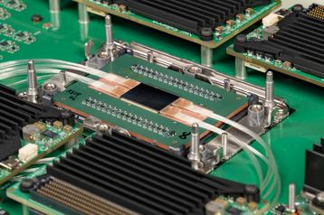
Salience Labs has already made strides to get its technology out of the lab and into actual deployment. Its all-optical 32-port switch debuted in the spring, with hardware testing giant Keysight brought on shortly after to validate the switching platform for use in AI data center infrastructure.
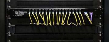
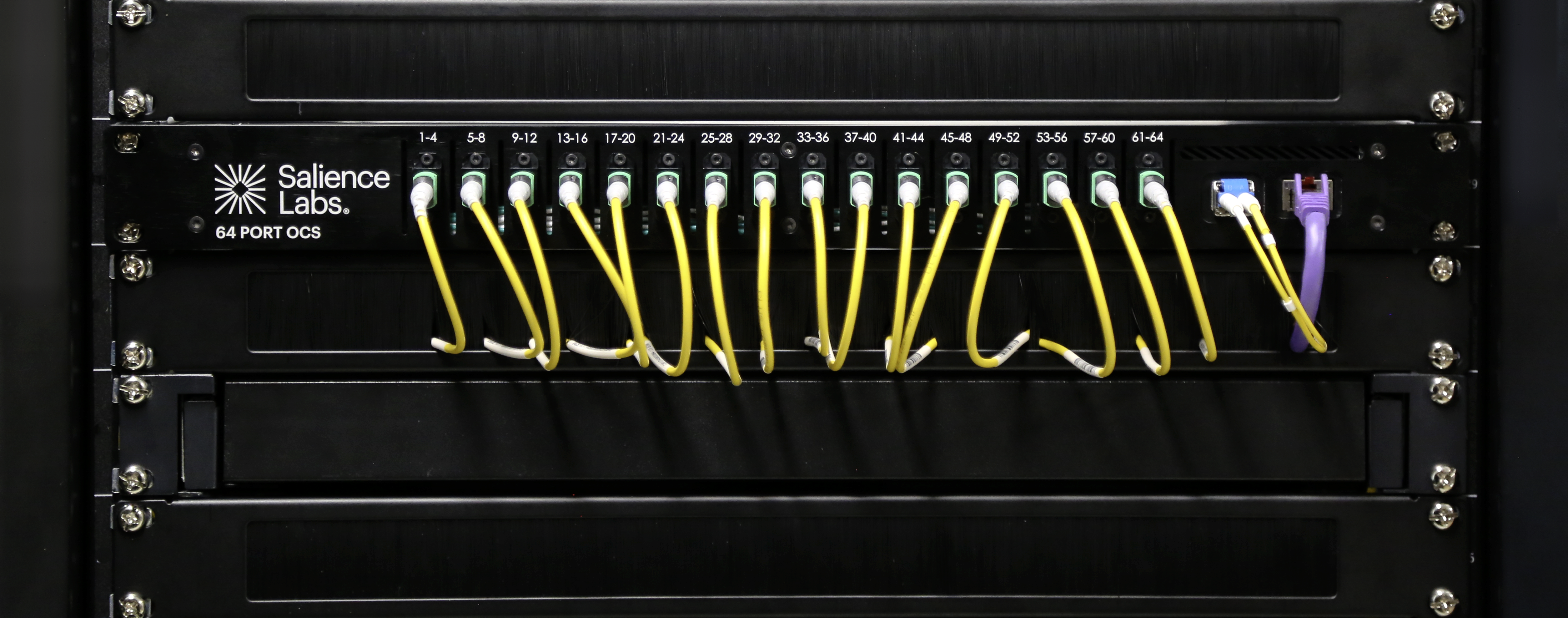
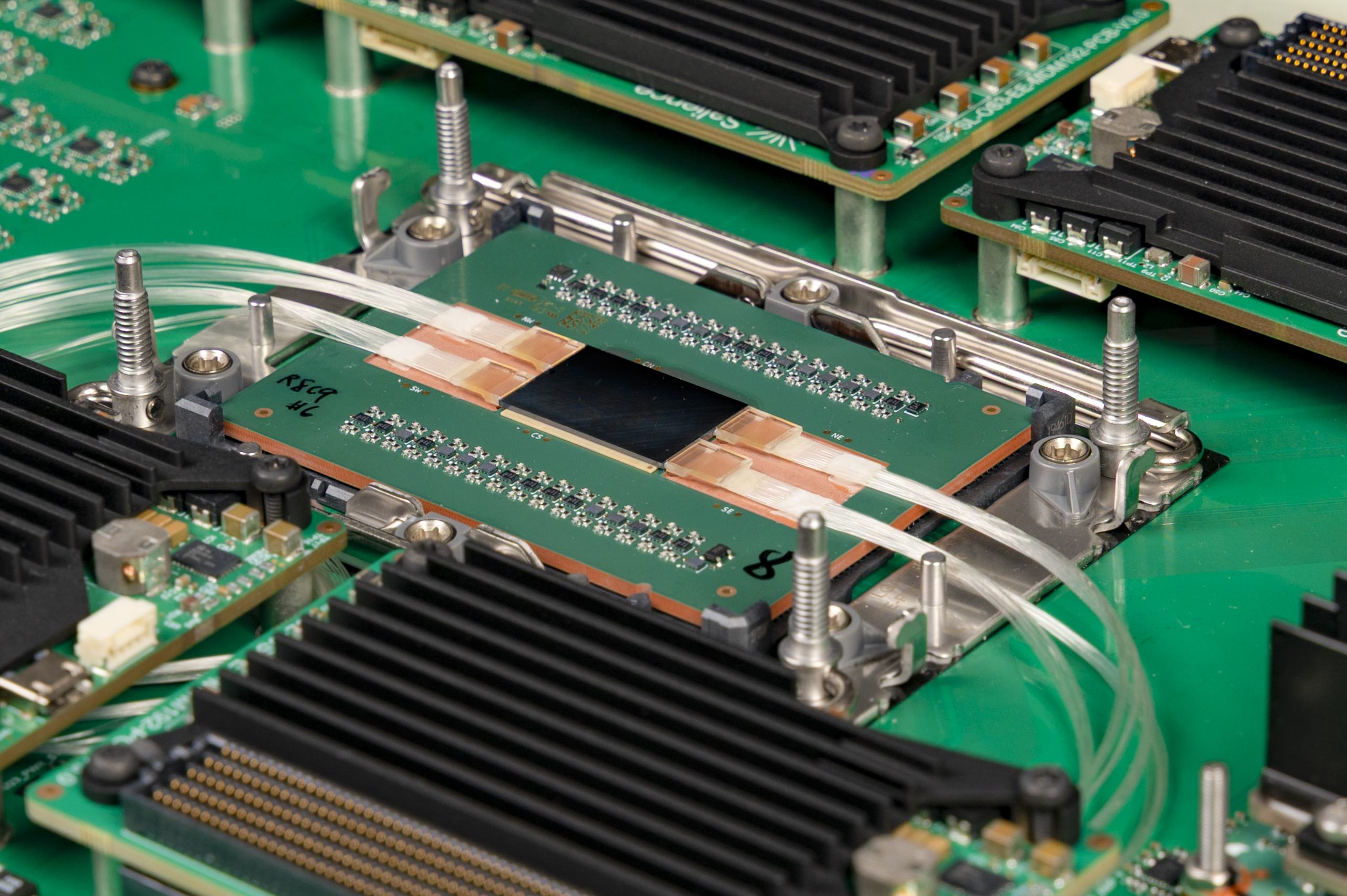
In late September, the startup unveiled the next iteration, shifting upward to 64 ports, of which SDxCentral was the first press outlet to look inside the box. And yet in chip size, it’s actually smaller than its predecessor owing to some serious design optimizations.
The switch is a standard one-rack-unit (1U) server box. And inside the box, compared to rival switches, Salience’s penchant for shrinking device size means engineers can fit multiple modules in a single box.
“You don't have to worry as much about thermals because it consumes very little power, which means you get to very good density,” Kewada explained.
While the startup is looking to expand across the pond, on the technology side, it plans to increase the port count per switch with a view to 128- and 256-port configurations – numbers that could potentially smash the current 72-GPU count stuck in scale-up configuration.
“We’re really at the beginning of what's possible in photonics; it is a green field space,” Kewada suggested. “Up until today, if you're fabricating silicon photonics, you're fabricating it on foundry processes that were designed for transceivers. What we've done is we've gone ahead and done from scratch the component design, in some cases even process changes, for optical circuit switches to do thousands of components onto a chip or multiples of that. And as a result of it, it's like we're at the very beginning of what's possible in silicon photonics.”






Comments